YM2612 register reference
Some explanation first. YM2612 has two sets of registers split in banks:
bank 0 is accessed at $A04000/1 and bank 1 is accessed at
$A04002/3. Registers come in three flavors: global,
per-channel and per-operator. In the latter two cases, bank 0 is for
the first three channels, and bank 1 is for the last three channels.
Meanwhile, global registers only exist in bank 0.
For some reason, register order is different from operator order (registers come in S1, S3, S2, S4 order), which leads to a lot of confusion. This page is using operator names taken from the YM3438 datasheet. When it comes to programming a sound driver, it's usually easier to process them in register order (the YM2612 doesn't care as long as it gets the correct values in the correct registers).
Also you may notice discrepancies with the official documentation. This is because Sega documented the values as if they were for 8MHz, while the YM2612 is actually connected to a slighly slower clock (specifically, the same one that feeds the 68000, which is 7.67MHz in NTSC and 7.61MHz in PAL). This page tries to use the corrected values.
$22: low frequency oscillator$24,$25: timer A frequency$26: timer B frequency$27: channel 3 mode and timer control$28: key-on and key-off$2A: DAC output$2B: DAC enable$30+:MUL(multiply) andDT(detune)$40+:TL(total level)$50+:AR(attack rate) andRS(rate scaling)$60+:DR(decay rate) and AM enable$70+:SR(sustain rate)$80+:RR(release rate) andSL(sustain level)$90+: SSG-EG$A0+: frequency$B0+: algorithm and feedback$B4+: panning, PMS, AMS
$22: low frequency oscillator
This is a global register. Its format is:
| Bit 7 | Bit 6 | Bit 5 | Bit 4 | Bit 3 | Bit 2 | Bit 1 | Bit 0 |
|---|---|---|---|---|---|---|---|
0
| 0
| 0
| 0
| LFOEN
| LFO:2
| LFO:1
| LFO:0
|
LFO: LFO frequencyLFOEN: 1 to turn on the LFO
The low frequency oscillator (LFO) is used to enable FMS and AMS to work for some simple vibrato- and tremolo-like effects. When the LFO is enabled, the following frequencies are available:
| Value | LFO frequency |
|---|---|
000 | 3.82 Hz |
001 | 5.33 Hz |
010 | 5.77 Hz |
011 | 6.11 Hz |
100 | 6.60 Hz |
101 | 9.23 Hz |
110 | 46.11 Hz |
111 | 69.22 Hz |
$24,$25: timer A frequency
These are global registers. Their format is:
| Bit 7 | Bit 6 | Bit 5 | Bit 4 | Bit 3 | Bit 2 | Bit 1 | Bit 0 |
|---|---|---|---|---|---|---|---|
TMRA:9
| TMRA:8
| TMRA:7
| TMRA:6
| TMRA:5
| TMRA:4
| TMRA:3
| TMRA:2
|
| Bit 7 | Bit 6 | Bit 5 | Bit 4 | Bit 3 | Bit 2 | Bit 1 | Bit 0 |
|---|---|---|---|---|---|---|---|
0
| 0
| 0
| 0
| 0
| 0
| TMRA:1
| TMRA:0
|
TMRA: timer A frequency
Timer A counts from TMRA to $400 (when it
"overflows"), then reloads and repeats. The exact frequency is computed
as follows (approximately):
($400 - TMRA) × 18.77µs
$26: timer B frequency
This is a global register. Its format is:
| Bit 7 | Bit 6 | Bit 5 | Bit 4 | Bit 3 | Bit 2 | Bit 1 | Bit 0 |
|---|---|---|---|---|---|---|---|
TMRB:7
| TMRB:6
| TMRB:5
| TMRB:4
| TMRB:3
| TMRB:2
| TMRB:1
| TMRB:0
|
TMRB: timer B frequency (higher = faster)
Timer B counts from TMRB to $100 (when it
"overflows"), then reloads and repeats. The exact frequency is computed
as follows (approximately):
($100 - TMRB) × 300.34µs
$27: channel 3 mode and timer control
This is a global register. Its format is:
| Bit 7 | Bit 6 | Bit 5 | Bit 4 | Bit 3 | Bit 2 | Bit 1 | Bit 0 |
|---|---|---|---|---|---|---|---|
MODE:1
| MODE:0
| RST:B
| RST:A
| ENBL:B
| ENBL:A
| LOAD:B
| LOAD:A
|
LOAD: controls whether the respective timer runs- 0: timer is frozen
- 1: timer is running
ENBL: determines what happens when the respective timer overflows- 0: does nothing
- 1: sets the flag
RST: modifies the respective timer flag when reading from$A04000- 0: leave it as-is
- 1: clear the flag
MODE: channel 3 mode00: normal (like the other channels)01: special (each operator has its own frequency)10: CSM
Quick guide to using the timers (if you just want to let them run and check when they fire, which is probably the only thing you'll need):
| Value | Timers | ch3 mode |
|---|---|---|
$0F | — | Normal |
$1F | Acknowledge timer A | Normal |
$2F | Acknowledge timer B | Normal |
$3F | Acknowledge both timers | Normal |
$4F | — | Special |
$5F | Acknowledge timer A | Special |
$6F | Acknowledge timer B | Special |
$7F | Acknowledge both timers | Special |
$28: key-on and key-off
This is a global register. Its format is:
| Bit 7 | Bit 6 | Bit 5 | Bit 4 | Bit 3 | Bit 2 | Bit 1 | Bit 0 |
|---|---|---|---|---|---|---|---|
OPERS3
| OPERS2
| OPERS1
| OPERS0
| 0
| CH:2
| CH:1
| CH:0
|
CH: which channelOPERS0: operator S1 (0 = key-off, 1 = key-on)OPERS1: operator S2 (0 = key-off, 1 = key-on)OPERS2: operator S3 (0 = key-off, 1 = key-on)OPERS3: operator S4 (0 = key-off, 1 = key-on)
The first three channels are 000-010, the last three
channels are 100-110.
Each operator can be set separately, but you'll usually set them all the same way. Attack rate starts when going from off to on, release rate starts when going from on to off. Envelope is not affected when staying the same.
$2A: DAC output
This is a global register. When DAC output is enabled, the value written here is output as-is on the 6th channel. To play PCM sound you need to be constantly writing to this register at the exact moment the samples are meant to be output (oof).
$2B: DAC enable
This is a global register. Its format is:
| Bit 7 | Bit 6 | Bit 5 | Bit 4 | Bit 3 | Bit 2 | Bit 1 | Bit 0 |
|---|---|---|---|---|---|---|---|
DACEN
| 0
| 0
| 0
| 0
| 0
| 0
| 0
|
DACEN: 6th channel output- 0: output FM
- 1: output DAC
$30+: MUL (multiply) and DT (detune)
This register exists per-operator:
| Channel | Oper S1 | Oper S2 | Oper S3 | Oper S4 |
|---|---|---|---|---|
| 1st/4th | $30 | $38 | $34 | $3C
|
| 2nd/5th | $31 | $39 | $35 | $3D
|
| 3rd/6th | $32 | $3A | $36 | $3E
|
The register format is:
| Bit 7 | Bit 6 | Bit 5 | Bit 4 | Bit 3 | Bit 2 | Bit 1 | Bit 0 |
|---|---|---|---|---|---|---|---|
0
| DT:2
| DT:1
| DT:0
| MUL:3
| MUL:2
| MUL:1
| MUL:0
|
MUL: multiplierDT: detune
The MUL field specifies by how much the base frequency is
multiplied (by 1, 2, 3… up to 15). The exception to the rule is if this
value is 0, in which case it multiplies by 0.5 (i.e. halves the
frequency).
The DT field specifies a frequency detune, as follows (where
E is a small value that depends on the exact tone):
| Value | Detune |
|---|---|
000 | No detune |
001 | +1 × E |
010 | +2 × E |
011 | +3 × E |
100 | No detune |
101 | -1 × E |
110 | -2 × E |
111 | -3 × E |
$40+: TL (total level)
This register exists per-operator:
| Channel | Oper S1 | Oper S2 | Oper S3 | Oper S4 |
|---|---|---|---|---|
| 1st/4th | $40 | $48 | $44 | $4C
|
| 2nd/5th | $41 | $49 | $45 | $4D
|
| 3rd/6th | $42 | $4A | $46 | $4E
|
The register format is:
| Bit 7 | Bit 6 | Bit 5 | Bit 4 | Bit 3 | Bit 2 | Bit 1 | Bit 0 |
|---|---|---|---|---|---|---|---|
0
| TL:6
| TL:5
| TL:4
| TL:3
| TL:2
| TL:1
| TL:0
|
TL: total level (every step is 0.75dB quieter)
Total level is what is normally thought of as the "volume". If you want
to affect the volume of a channel, make sure to only touch the
TL of "slot" (output) operators and not those that feed
into other operators.
$50+: AR (attack rate) and RS (rate scaling)
This register exists per-operator:
| Channel | Oper S1 | Oper S2 | Oper S3 | Oper S4 |
|---|---|---|---|---|
| 1st/4th | $50 | $58 | $54 | $5C
|
| 2nd/5th | $51 | $59 | $55 | $5D
|
| 3rd/6th | $52 | $5A | $56 | $5E
|
The register format is:
| Bit 7 | Bit 6 | Bit 5 | Bit 4 | Bit 3 | Bit 2 | Bit 1 | Bit 0 |
|---|---|---|---|---|---|---|---|
RS:1
| RS:0
| 0
| AR:4
| AR:3
| AR:2
| AR:1
| AR:0
|
AR: attack rate (higher = steeper)RS: rate scaling
Rate scaling makes envelopes steeper at higher frequencies (needed to recreate how some instruments change sound as pitch becomes higher). A rate scaling of 0 does nothing, higher values increase this effect.
$60+: DR (decay rate) and AM enable
This register exists per-operator:
| Channel | Oper S1 | Oper S2 | Oper S3 | Oper S4 |
|---|---|---|---|---|
| 1st/4th | $60 | $68 | $64 | $6C
|
| 2nd/5th | $61 | $69 | $65 | $6D
|
| 3rd/6th | $62 | $6A | $66 | $6E
|
The register format is:
| Bit 7 | Bit 6 | Bit 5 | Bit 4 | Bit 3 | Bit 2 | Bit 1 | Bit 0 |
|---|---|---|---|---|---|---|---|
AMON
| 0
| 0
| DR:4
| DR:3
| DR:2
| DR:1
| DR:0
|
DR: decay rate (higher = steeper)AMON: 1 to let AMS affect this operator
Sometimes also called "first decay rate" (D1R).
$70+: SR (sustain rate)
This register exists per-operator:
| Channel | Oper S1 | Oper S2 | Oper S3 | Oper S4 |
|---|---|---|---|---|
| 1st/4th | $70 | $78 | $74 | $7C
|
| 2nd/5th | $71 | $79 | $75 | $7D
|
| 3rd/6th | $72 | $7A | $76 | $7E
|
The register format is:
| Bit 7 | Bit 6 | Bit 5 | Bit 4 | Bit 3 | Bit 2 | Bit 1 | Bit 0 |
|---|---|---|---|---|---|---|---|
0
| 0
| 0
| SR:4
| SR:3
| SR:2
| SR:1
| SR:0
|
SR: sustain rate (higher = steeper)
Sometimes also called "second decay rate" (D2R).
$80+: RR (release rate) and SL (sustain level)
This register exists per-operator:
| Channel | Oper S1 | Oper S2 | Oper S3 | Oper S4 |
|---|---|---|---|---|
| 1st/4th | $80 | $88 | $84 | $8C
|
| 2nd/5th | $81 | $89 | $85 | $8D
|
| 3rd/6th | $82 | $8A | $86 | $8E
|
The register format is:
| Bit 7 | Bit 6 | Bit 5 | Bit 4 | Bit 3 | Bit 2 | Bit 1 | Bit 0 |
|---|---|---|---|---|---|---|---|
SL:3
| SL:2
| SL:1
| SL:0
| RR:3
| RR:2
| RR:1
| RR:0
|
RR: release rate (higher = steeper)SL: sustain level (higher = at a quieter level)
Release rate has one bit less than the other rates.
Sustain level is at the point in the envelope where it switches from the first to the second decay rate. 0 is the peak of the envelope, 15 is the bottom of the envelope.
$90+: SSG-EG
This register is often incorrectly implemented in inaccurate clones and if you're unlucky they'll result in awful noise. If you really want to support those make sure to set this register to 0 in those cases.
This register exists per-operator:
| Channel | Oper S1 | Oper S2 | Oper S3 | Oper S4 |
|---|---|---|---|---|
| 1st/4th | $90 | $98 | $94 | $9C
|
| 2nd/5th | $91 | $99 | $95 | $9D
|
| 3rd/6th | $92 | $9A | $96 | $9E
|
The register format is:
| Bit 7 | Bit 6 | Bit 5 | Bit 4 | Bit 3 | Bit 2 | Bit 1 | Bit 0 |
|---|---|---|---|---|---|---|---|
0
| 0
| 0
| 0
| SSGEG:EN
| SSGEG:2
| SSGEG:1
| SSGEG:0
|
SSGEG: envelope shape
When SSGEG:EN is clear, nothing unusual happens. When it's
set, the envelope is processed in different ways (e.g. looping) depending
on what values the SSGEG:2-0 bits have. You must
make sure that attack rate is 31 or it will not
work properly.
SSGEG:2-0 | Envelope |
|---|---|
000 | 
|
001 | 
|
010 | 
|
011 | 
|
100 | 
|
101 | 
|
110 | 
|
111 | 
|
$A0+: frequency
These registers exists per channel:
| Channel | High half | Low half |
|---|---|---|
| 1st/4th | $A4 | $A0
|
| 2nd/5th | $A5 | $A1
|
| 3rd/6th | $A6 | $A2
|
When in channel 3 special mode, the third FM channel (but not the sixth) can have its frequency set per operator. In this case, the registers for channel 3 are as follows:
| Operator | High half | Low half |
|---|---|---|
| S1 | $AD | $A9
|
| S2 | $AE | $AA
|
| S3 | $AC | $A8
|
| S4 | $A6 | $A2
|
The registers format is:
| Bit 7 | Bit 6 | Bit 5 | Bit 4 | Bit 3 | Bit 2 | Bit 1 | Bit 0 |
|---|---|---|---|---|---|---|---|
0
| 0
| BLK:2
| BLK:1
| BLK:0
| FREQ:10
| FREQ:9
| FREQ:8
|
| Bit 7 | Bit 6 | Bit 5 | Bit 4 | Bit 3 | Bit 2 | Bit 1 | Bit 0 |
|---|---|---|---|---|---|---|---|
FREQ:7
| FREQ:6
| FREQ:5
| FREQ:4
| FREQ:3
| FREQ:2
| FREQ:1
| FREQ:0
|
FREQ: frequencyBLK: block (octave)
To set the frequency, first write its higher half then its lower half (frequency won't be updated until the latter write).
The block acts like the octave: frequency is doubled every time it's incremented by 1. As for the frequency, here are some approximate values (as used by Echo), though they're off by a bit depending on whether it's a NTSC or PAL system:
| Semitone | Frequency |
|---|---|
| C | 644 |
| C# | 681 |
| D | 722 |
| D# | 765 |
| E | 810 |
| F | 858 |
| F# | 910 |
| G | 964 |
| G# | 1021 |
| A | 1081 |
| A# | 1146 |
| B | 1214 |
$B0+: algorithm and feedback
This register exists per channel:
| Channel | Register |
|---|---|
| 1st/4th | $B0
|
| 2nd/5th | $B1
|
| 3rd/6th | $B2
|
The register format is:
| Bit 7 | Bit 6 | Bit 5 | Bit 4 | Bit 3 | Bit 2 | Bit 1 | Bit 0 |
|---|---|---|---|---|---|---|---|
0
| 0
| FEED:2
| FEED:1
| FEED:0
| ALGO:2
| ALGO:1
| ALGO:0
|
ALGO: algorithmFEED: channel 1 feedback
The algorithm describes which operators modulate other operators, and which operators generate the final output. Different algorithms can generate wildly different sounds. The are eight available arrangements.
| Algorithm | Arrangement |
|---|---|
0 (000) | 
|
1 (001) | 
|
2 (010) | 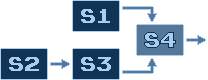
|
3 (011) | 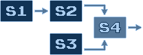
|
4 (100) | 
|
5 (101) | 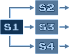
|
6 (110) | 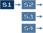
|
7 (111) | 
|
Operator S1 can modulate itself (on top of the algorithm's arrangement),
FEED controls how much it does so. 0 is no feedback, higher
values increase the self-modulation.
$B4+: panning, PMS, AMS
This register exists per channel:
| Channel | Register |
|---|---|
| 1st/4th | $B4
|
| 2nd/5th | $B5
|
| 3rd/6th | $B6
|
The register format is:
| Bit 7 | Bit 6 | Bit 5 | Bit 4 | Bit 3 | Bit 2 | Bit 1 | Bit 0 |
|---|---|---|---|---|---|---|---|
L
| R
| AMS:1
| AMS:0
| 0
| PMS:2
| PMS:1
| PMS:0
|
L: 1 to output to left speakerR: 1 to output to right speakerAMS: amplitude modulation sensivityPMS: frequency modulation sensivity
Frequency and amplitude sensivity (PMS and AMS respectively) are meant to be used together with the LFO and indicate how much is the waveform affected by it.
PMS can be used as a cheap form of vibrato. The values are:
| Value | Modulation |
|---|---|
000 | None |
001 | ±0.034 semitones |
010 | ±0.067 semitones |
011 | ±0.10 semitones |
100 | ±0.14 semitones |
101 | ±0.20 semitones |
110 | ±0.40 semitones |
111 | ±0.80 semitones |
AMS only affects those operators where the AM bit has been set, and it can be used as a cheap form
of tremolo. The possible values are:
| Value | Modulation |
|---|---|
00 | None |
01 | ±1.4 dB |
10 | ±5.9 dB |
11 | ±11.8 dB |
Iwis says
PMS actually stands for "phase modulation
sensivity" (since the YM2612 actually does phase modulation instead of
frequency modulation). The outcome is more or less the same, aside from
rounding errors.